← NEMA L6-20P Wiring Diagram – Safe & Efficient Power! Nema 6 20p wiring diagram Puppies and Kitties 3: The Cutest Viral Trend Yet! The three cutest kittens stock illustration. illustration of poses ... →
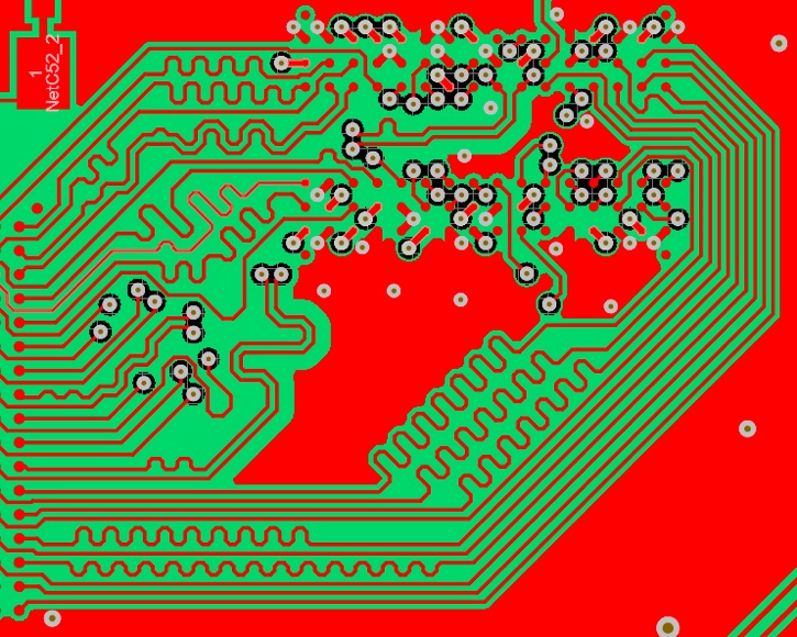
If you are searching about Main Design Guidelines & Layout Rules on High Speed PCB you've visit to the right web. We have 25 Images about Main Design Guidelines & Layout Rules on High Speed PCB like Some LVDS PCB Layout Guidelines For Ensuring Signal, 40% OFF, Some LVDS PCB Layout Guidelines For Ensuring Signal, 40% OFF and also Main Design Guidelines & Layout Rules on High Speed PCB. Read more:
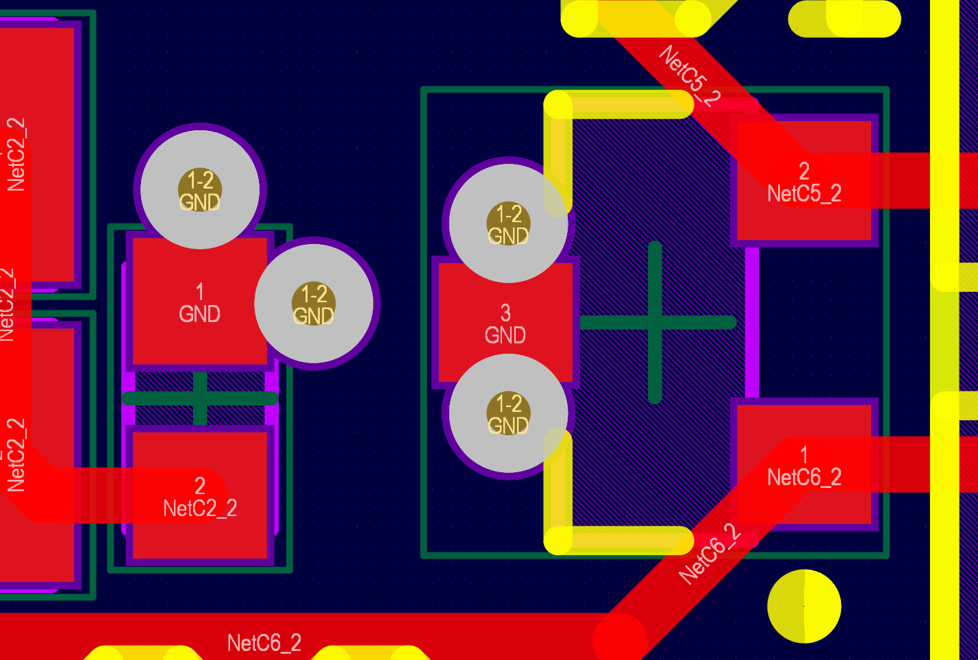
Main Design Guidelines & Layout Rules On High Speed PCB
 www.integrasources.com
Main Design Guidelines & Layout Rules on High Speed PCB
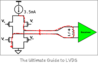
Some LVDS PCB Layout Guidelines For Ensuring Signal, 40% OFF
 www.oceanproperty.co.th
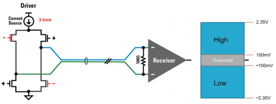
Some LVDS PCB Layout Guidelines For Ensuring Signal, 40% OFF
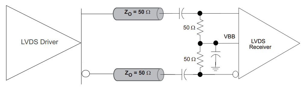
Some LVDS PCB Layout Guidelines For Ensuring Signal Integrity | PCB
 resources.altium.com
Some LVDS PCB Layout Guidelines for Ensuring Signal Integrity | PCB ...
PCB Layout Guidelines And Considerations
 www.microcontrollertips.com
PCB layout guidelines and considerations
Pcb Layout Guidelines Top 5 Pcb Design Rules You Need To Know
 electricalcircuit.z6.web.core.windows.net
pcb layout guidelines Top 5 pcb design rules you need to know
Motor-Driver PCB Layout Guidelines (Part 1) | Electronic Design
 www.electronicdesign.com
Motor-Driver PCB Layout Guidelines (Part 1) | Electronic Design
LVDS Board Design Guidelines: Altera FPGAs & PCB Layout
 studylib.net
studylib.net
LVDS Board Design Guidelines: Altera FPGAs & PCB Layout
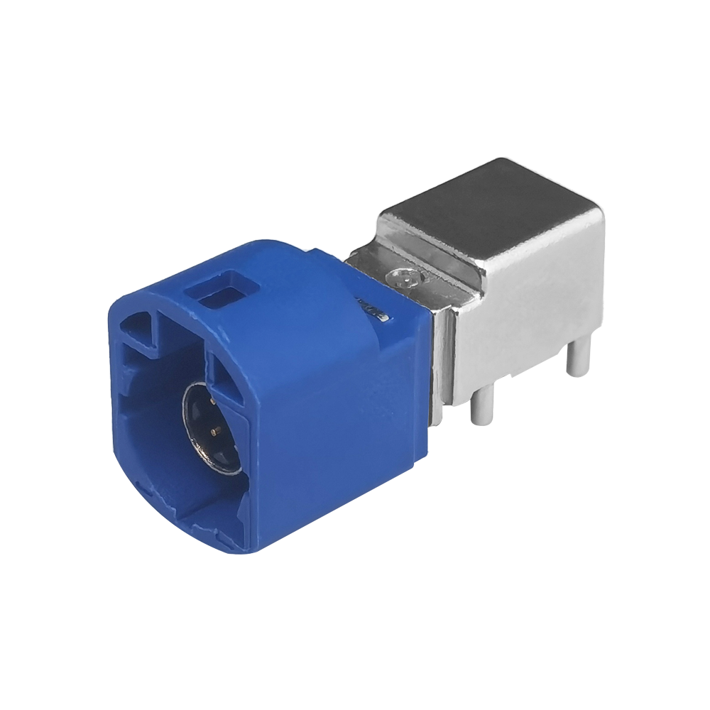
Limited Edition FAKRA HSD LVDS PCB Mount RF Connector
 content.fakraconnectors.com
Limited Edition FAKRA HSD LVDS PCB Mount RF Connector
High Speed Pcb Design Guidelines - Design Talk
 design.udlvirtual.edu.pe
High Speed Pcb Design Guidelines - Design Talk
High Speed Pcb Layout Guidelines - Design Talk
 design.udlvirtual.edu.pe
High Speed Pcb Layout Guidelines - Design Talk
Some LVDS PCB Layout Guidelines For Ensuring Signal Integrity | PCB
 resources.altium.com
Some LVDS PCB Layout Guidelines for Ensuring Signal Integrity | PCB ...
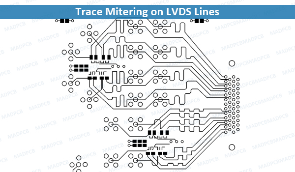
LVDS: High Speed LVDS PCB Design Guidelines | MADPCB
 madpcb.com
LVDS: High Speed LVDS PCB Design Guidelines | MADPCB
Component Placement In PCB Design & Assembly | Sierra Circuits
 www.protoexpress.com
Component Placement in PCB Design & Assembly | Sierra Circuits
Some LVDS PCB Layout Guidelines For Ensuring Signal Integrity | PCB
 resources.altium.com
Some LVDS PCB Layout Guidelines for Ensuring Signal Integrity | PCB ...
Some LVDS PCB Layout Guidelines For Ensuring Signal, 40% OFF
 www.oceanproperty.co.th
Some LVDS PCB Layout Guidelines For Ensuring Signal, 40% OFF
PCB Layout Guidelines For USB Type-C
PCB Layout Guidelines for USB Type-C
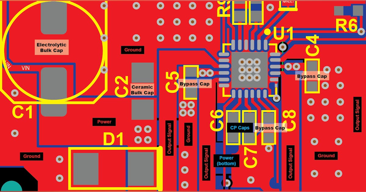
Switched-Mode Power Supply PCB Design Guidelines | Altium
 resources.altium.com
Switched-Mode Power Supply PCB Design Guidelines | Altium
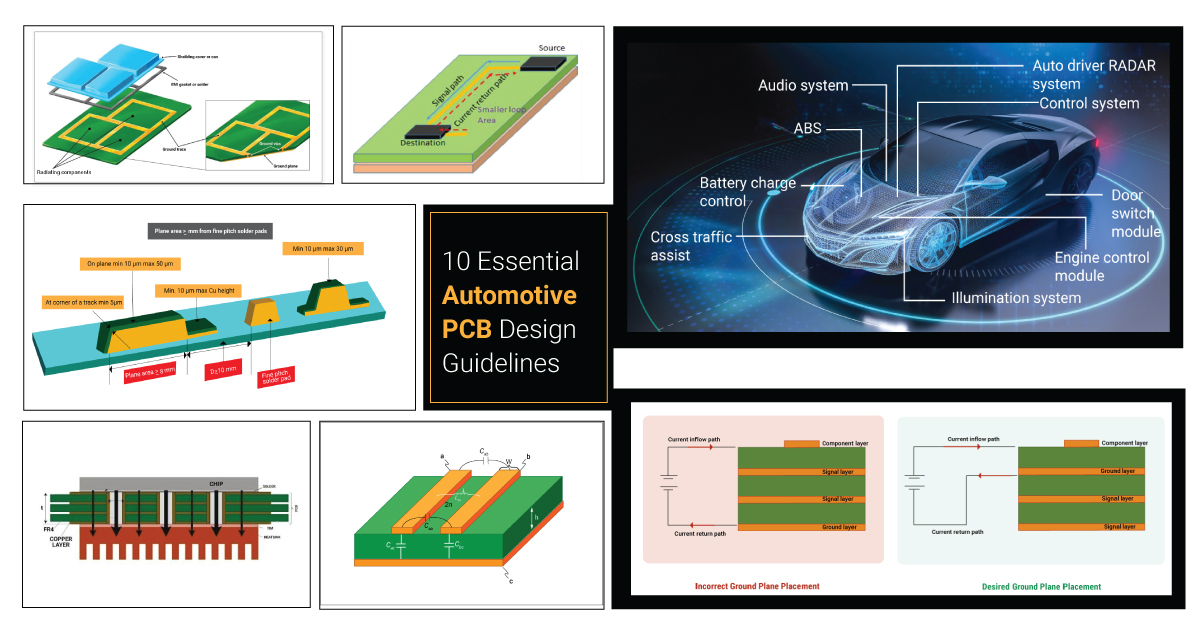
10 Automotive PCB Design Guidelines | Sierra Circuits
 www.protoexpress.com
10 Automotive PCB Design Guidelines | Sierra Circuits
Some LVDS PCB Layout Guidelines For Ensuring Signal Integrity | PCB
 resources.altium.com
Some LVDS PCB Layout Guidelines for Ensuring Signal Integrity | PCB ...
Reparator Credential Dumnezeu Pcb Design Guidelines Releu Alb Ca
 cristor.dz
Reparator Credential Dumnezeu pcb design guidelines releu alb ca ...
High Current Pcb Design Guidelines - Design Talk
 design.udlvirtual.edu.pe
High Current Pcb Design Guidelines - Design Talk
Some LVDS PCB Layout Guidelines For Ensuring Signal Integrity | PCB
Some LVDS PCB Layout Guidelines for Ensuring Signal Integrity | PCB ...
Pcb Design Differential Impedance Of Lvds Rules And T - Vrogue.co
 www.vrogue.co
Pcb Design Differential Impedance Of Lvds Rules And T - vrogue.co
Some LVDS PCB Layout Guidelines For Ensuring Signal Integrity | PCB
Some LVDS PCB Layout Guidelines for Ensuring Signal Integrity | PCB ...
Pcb Layout Guidelines Can Bus Pcb Circuits – Eroppa
 eroppa.com
Pcb Layout Guidelines Can Bus Pcb Circuits – Eroppa
Some lvds pcb layout guidelines for ensuring signal, 40% off. Main design guidelines & layout rules on high speed pcb. High current pcb design guidelines